
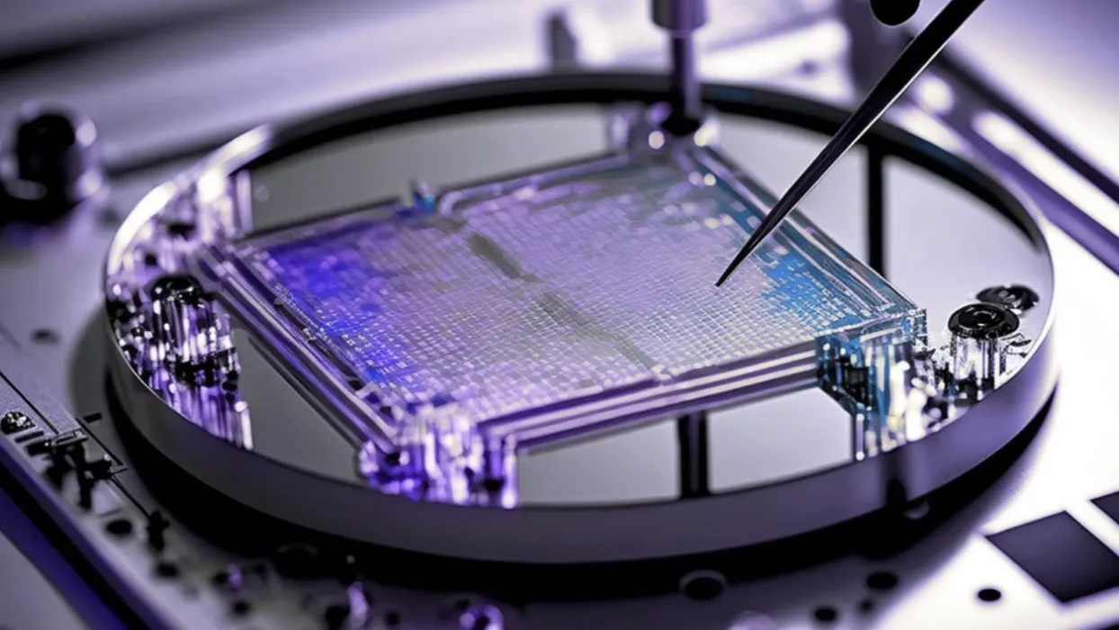
Tools created to extend Moore’s Law may find a new life far beyond their original mission. As the quantum computing field develops, it is becoming clear that many of its most promising architectures, including photon-based systems, will require a level of patterning precision that only the semiconductor industry can deliver. Erik Hosler, a panelist involved in patterning strategies for next-generation computing platforms, made the case at the SPIE Advanced Lithography symposium. Techniques originally designed for scaling classical logic may be just what quantum needs next.
This convergence is not theoretical. It is already happening. Researchers exploring photonic quantum processors are beginning to use advanced lithography tools, including Extreme Ultraviolet (EUV) systems, to define critical structures. The same alignment tolerances, etch profiles, and defect mitigation practices developed for classical chips now appear essential for building scalable, stable quantum platforms. If quantum photonics is to succeed, it will do so by borrowing heavily from the infrastructure of classical scaling.
Semiconductor Tools, Quantum Targets
For years, EUV was viewed as the savior of classical semiconductor scaling. Its ability to produce features smaller than conventional DUV systems helped extend transistor density and delay the limits of two-dimensional logic. Now, the same capabilities are being repurposed for something quite different: defining the physical geometry of photonic quantum components.
Unlike superconducting or spin-based systems, photon-based quantum platforms rely on light, not charge or magnetism, to carry information. These systems require precise manipulation of waveguides, resonators, phase shifters, and beam splitters, all built with nanometer-level alignment. The optical paths must be stable across chips and wafers. Even the slightest irregularity in width or curvature can degrade quantum interference, the foundation of photonic entanglement and logic.
In this context, classical patterning tools are useful and indispensable. Fabrication teams now find themselves applying EUV machines, resist stacks, and proximity correction models to shape waveguide structures instead of gate electrodes. The underlying challenge is the same: Pattern light. Then, make it work.
Why EUV Might Be the Unexpected Hero
The shift in purpose was highlighted clearly during the SPIE panel session. “Patterning techniques developed for advanced EUV… might be needed in a photon-based quantum computer,” Erik Hosler shares. It reflects a growing awareness within both industries. Tools built for one domain may become essential in another. The high-precision exposure systems and resist processes that enabled 7 nm and 5 nm logic nodes may also make scalable photonic qubit arrays possible.
That is because quantum photonics demands extreme spatial regularity. The waveguides and splitters on these chips must function identically across hundreds or thousands of instances. Variability introduces phase noise and limits the system’s ability to maintain interference conditions. These chips must perform like optics, not electronics. Uniformity is not just preferred. It is required.
EUV lithography, with its short wavelength and high alignment accuracy, offers a direct solution. It can define features that allow photonic elements to be tightly packed without crosstalk. It can also deliver uniformity across wafer-scale chips, supporting the kind of integration needed for fault-tolerant quantum processors. Hosler’s point reframes EUV not as an endgame for classical chips but as a stepping stone for something entirely new. The tool is the same, but the outcome is different.
From Scaling Logic to Sculpting Light
Photon-based quantum computers process information using entangled states of light. This architecture requires a completely different hardware structure than that used for electronic qubits. Gratings, interferometers, and multiplexed waveguides become the core computational units. Their performance depends on their exact size, shape, and optical path length.
To make this work, designers need tools that can etch curves, align across layers, and control sidewall profiles with precision. The same demands that once drove the development of multi-patterning, EUV masks, and high-resolution resists are now being reapplied. But instead of driving logic through, they now enable coherence, interference, and entanglement.
Many of the early quantum photonic devices were handcrafted, with high variability between runs. That approach was suitable for research but not for scale. The adoption of lithography-grade patterning is changing that. Wafer-scale runs of photonic quantum chips are now becoming possible. The designs are growing more complex, with dense optical routing and hybrid integration with control electronics. EUV may not have been built for this task. But it appears uniquely suited to it.
Patterning Precision Across Domains
The themes discussed during the SPIE panel point to a common thread. Whether building logic gates or qubit arrays, the demands on patterning are converging. Stochastic defects, resist blur, line edge roughness, and etch bias are challenges in both classical and quantum domains.
In classical chips, those problems affect performance and yield. In quantum chips, they affect physical function. A rough waveguide edge changes the path of a photon, and a slight etch inconsistency shifts the phase of an optical pulse. These are not minor variations, but system-breaking defects.
That is why the best practices from semiconductor patterning now matter more than ever. Precision resist processing, calibrated exposure, and multi-pass inspection are becoming standard in quantum workflows. The defect tolerances may be tighter. But the principle is the same. Pattern once. Get it right.
The overlap goes even further. Multi-layer integration, heterogeneous materials, and advanced packaging are also shared challenges. The difference is that in quantum, the tolerances are more severe, and the fallback options are fewer. For many photonic platforms, fabrication determines feasibility.
EUV’s Second Act Begins with Quantum
There was a time when the EUV represented the bleeding edge of classical chipmaking. It marked the last stretch of lithographic scaling before new materials and 3D structures took over. But now, EUV is entering a second phase. One that may prove just as impactful.
As quantum platforms push toward scalability, the need for stable, uniform, high-resolution patterning has become unavoidable. Photonic systems require proven tools, and EUV is at the top of that list. The broader message is clear. Quantum will not be built from scratch. It will be built from the same tools that shaped the past two decades of computing. Those tools may find new purpose, serving new architectures and new goals.
If photon-based quantum computers become a reality, it will not be because of some mysterious leap. It will be because existing technology has been put to a new use. EUV’s most significant role may not be extending Moore’s Law. It may be enabling what comes after it.
